

Silicon Wafer
OST Photonics offers a wide selection of silicon wafers for semiconductor industry. The wafer diameters are ranging from 2 inch (50.8mm) to 12 inch...
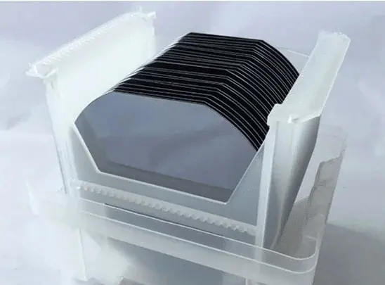
Silicon Wafer
OST Photonics offers a wide selection of silicon wafers for semiconductor industry. The wafer diameters are ranging from 2 inch (50.8mm) to 12 inch (300mm), and there are three crystal orientations to choose from: <100>, <111> and <110>, the thickness can also be customized according to your requirements. In addition, SOI wafers, oxide silicon wafers, customized silicon substrates and silicon ingots are also availabl...
- ManufacturerOST Photonics
- CategoryCrystal Wafer and Substrate
- Lead TimeQuoted per order
- CustomizationSize, orientation and surface finish to drawing
Silicon Wafer (Si Wafer)
Specifications of Czochralski (CZ) Silicon Wafers
| Item | Specifications | ||||||
| Diameter | 2″ | 3″ | 4″ | 5″ | 6″ | 8″ | 12″ |
| Grade | Prime grade, Test grade, Dummy grade | ||||||
| Growth Method | CZ | ||||||
| Orientation | <100>,<111>,<110>, etc. | ||||||
| Type/Dopant | P-type/Boron, N-type/Phos, N-type/As, N-type/Sb | ||||||
| Thickness (um) | 279 | 380 | 525 | 625 | 675 | 725 | 775 |
| Thickness Tolerance | Standard ±25um, Maximum Capabilities ±5um | ± 20um | ± 20um | ||||
| Resistivity(Ohm-cm) | 0.001-100 | ||||||
| Surface Finished | Polished/Etched, Polished/Polished, Etched/Etched, Ground/Ground | ||||||
| TTV (um) | Standard < 10um, Maximum Capabilities<5um | ||||||
| Bow/Warp (um) | Standard < 40um, Maximum Capabilities<20um | <40um | <40um | ||||
| Particle | Upon Request |
Specifications of Float Zone (FZ) Silicon Wafers
| Item | Specifications | |||||
| Diameter | 2″ | 3″ | 4″ | 5″ | 6″ | 8″ |
| Grade | Prime grade, Test grade, Dummy grade | |||||
| Growth Method | FZ | |||||
| Orientation | <100>,<111>, etc. | |||||
| Type/Dopant | Intrinsic, P-type/Boron, N-type/Phos | |||||
| Thickness (um) | 279 | 380 | 525 | 625 | 675 | 725 |
| Thickness Tolerance | Standard ±25um | ± 50um | ||||
| Resistivity(Ohm-cm) | 1000-30000 and 1-5 | |||||
| Surface Finished | Polished/Etched, Polished/Polished, Etched/Etched, Ground/Ground | |||||
| TTV (um) | Standard < 10um | |||||
| Bow/Warp (um) | Standard < 40um | <50um | ||||
| Particle | Upon Request |
Specifications of Oxide Silicon Wafers
| Item | Specifications | ||||||
| Diameter | 2″ | 3″ | 4″ | 5″ | 6″ | 8” | 12” |
| Grade | Prime grade, Test grade, Dummy grade | ||||||
| Growth Method | CZ, FZ | ||||||
| Orientation | <100>,<111>,<110>, etc. | ||||||
| Type/Dopant | Intrinsic, P-type/Boron, N-type/Phos, N-type/As, N-type/Sb | ||||||
| Thickness (um) | 279 | 380 | 525 | 625 | 675 | 725 | 775 |
| Thickness Tolerance | Standard ±25um, Maximum Capabilities ±5um | ± 20um | ± 20um | ||||
| Oxide Thickness (nm) | 20-2000 | ||||||
| Resistivity(Ohm-cm) | 0.001-30000 | ||||||
| Surface Finished | Polished/Etched, Polished/Polished | ||||||
| TTV (um) | Standard < 10um, Maximum Capabilities<5um | ||||||
| Bow/Warp (um) | Standard < 40um, Maximum Capabilities<20um | <40um | <40um | ||||
| Particle | Upon Request |
Specifications of Silicon Ingots
| Item | Specifications | |||||
| Diameter | 2″ | 3″ | 4″ | 5″ | 6″ | 8″ |
| Grade | Prime grade, Test grade, Dummy grade | |||||
| Growth Method | CZ, FZ | |||||
| Orientation | <100>,<111>,<110>, etc. | |||||
| Type/Dopant | Intrinsic, P-type/Boron, N-type/Phos, N-type/As, N-type/Sb | |||||
| Oxygen Content | 8-18 ppma | |||||
| Carbon Content | >1 ppma | |||||
| Resistivity(Ohm-cm) | 0.001-30000 ohm-cm | |||||
| Life Time | >50us |
Other Crystal Wafer and Substrate Materials


Request A Quote For Silicon Wafer
Send us your dimensions, orientation, surface finish and quantity. Our engineers reply with a technical proposal and price.
Buyer Questions
What is the item of the Silicon Wafer?
What is the grade of the Silicon Wafer?
What is the growth method of the Silicon Wafer?
What is the orientation of the Silicon Wafer?
How do I get a quotation for the Silicon Wafer?
Can the Silicon Wafer be made to a custom specification?
Who manufactures the Silicon Wafer?
Tell Us What You Need
Send your specification, quantity and destination port. Our engineers reply with a technical proposal and a confirmed lead time.