

ZnO Substrate
Zinc oxide (ZnO) is a good substrate for GaN thin film. It has a large exciton binding energy of 60 MeV and a bandwidth of 3.73 eV at room temperature,...
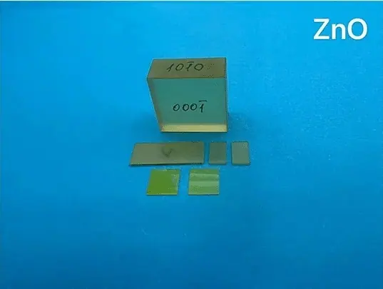
ZnO Substrate
Zinc oxide (ZnO) is a good substrate for GaN thin film. It has a large exciton binding energy of 60 MeV and a bandwidth of 3.73 eV at room temperature, making it a luminescent material for ultraviolet and visible light. Due to the transparency in the visible region, the large electromechanical coupling coefficient and the properties of adsorption and desorption of gas molecules on its surface, it is expected to be us...
- ManufacturerOST Photonics
- CategoryCrystal Wafer and Substrate
- Stock Items4 listed specifications
- Lead TimeQuoted per order
- CustomizationSize, orientation and surface finish to drawing
Zinc oxide (ZnO) is a good substrate for GaN thin film. It has a large exciton binding energy of 60 MeV and a bandwidth of 3.73 eV at room temperature, making it a luminescent material for ultraviolet and visible light. Due to the transparency in the visible region, the large electromechanical coupling coefficient and the properties of adsorption and desorption of gas molecules on its surface, it is expected to be used in energy limiters with high peak energy, GaN substrates with large size and high quality, and wireless communications which beyond 5GHz in the future, high electric field equipment, high temperature and high energy electronic devices, etc..
OST Photonics offers high quality ZnO substrates for researchers and industries. Crystal orientation, size and thickness can be customized according to your requirements.
Features
- Large exciton binding energy of 60 MeV
- Large bandwidth of 3.73 eV
- High transparency in the visible region
- Large electromechanical coupling coefficient
Applications
- Substrate for GaN thin film
- Wireless communications
- High temperature and high energy electronic devices
- High electric field equipment
Processing Capability
- Orientation: <0001>, <11-20>, <10-10>, etc.
- Dimension: 5x5mm, 10x10mm, 15x15mm, 20x20mm, 25x25mm, etc.
- Thickness: 0.5mm, 1.0mm, etc.
- Available items: substrates, blanks and customized optics
Specification and Properties of ZnO Substrates
| Crystal System | Hexagonal |
| Growth Method | Hydrothermal |
| Crystal Lattice Constant | a=3.252 Å c=5.313 Å |
| Melting Point | 1975 ℃ |
| Density | 5.7 g/cm3 |
| Hardness | 4 Mohs |
| Thermal Expansion Coefficient | //a: 6.5×10^-6 /℃ //c: 3.7×10^-6 /℃ |
| Specific Heat | 0.125 cal/g.m |
| Thermoelectric Constant | 1200 mv/k @ 300 ℃ |
| Heat Conductivity | 0.006 cal/cm/k |
| Transmission Range | >50%@0.4-0.6 um (2mm) |
| Orientation | <0001>,<11-20>,<10-10>, etc. |
| Orientation Tolerance | ±0.5° or better |
| Dimension | 5x5mm, 10x10mm, 15x15mm, 20x20mm, 25x25mm, etc. |
| Dimension Tolerance | ±0.1 mm or better |
| Thickness | 0.5mm, 1.0mm, etc. |
| Thickness Tolerance | ±0.05 mm or better |
| Surface Finish | Single side polished (SSP)/Double sides polished (DSP) |
| Surface Roughness | Ra<5Å (5µmx5µm) |
| Package | Class 100 clean bag, Class 1000 super clean room |
Available ZnO Substrate Items
The following specifications are listed on our original catalogue. Custom dimensions, orientations and surface finishes are produced to your drawing.
| 5 mm x 5 mm x 0.5 mm ZnO Single Crystal Substrates, Orientation: (100), Double Sides Polished (10 Pieces) | View |
| 5 mm x 5 mm x 0.5 mm ZnO Single Crystal Substrates, Orientation: (100), Single Side Polished (10 Pieces) | View |
| 10 mm x 10 mm x 0.5 mm ZnO Single Crystal Substrates, Orientation: (100), Double Sides Polished (5 Pieces) | View |
| 10 mm x 10 mm x 0.5 mm ZnO Single Crystal Substrates, Orientation: (100), Single Side Polished (5 Pieces) | View |
Other Crystal Wafer and Substrate Materials


Request A Quote For ZnO Substrate
Send us your dimensions, orientation, surface finish and quantity. Our engineers reply with a technical proposal and price.
Buyer Questions
What is the crystal system of the ZnO Substrate?
What is the growth method of the ZnO Substrate?
What is the crystal lattice constant of the ZnO Substrate?
What is the melting point of the ZnO Substrate?
How do I get a quotation for the ZnO Substrate?
Can the ZnO Substrate be made to a custom specification?
Who manufactures the ZnO Substrate?
Tell Us What You Need
Send your specification, quantity and destination port. Our engineers reply with a technical proposal and a confirmed lead time.