

BaF2 Substrate
Barium fluoride (BaF2) is a scintillation crystal known for its fast and slow emission components. It offers sub-nanosecond timing resolution, making it...
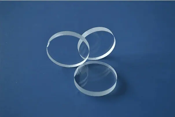
BaF2 Substrate
Barium fluoride (BaF2) is a scintillation crystal known for its fast and slow emission components. It offers sub-nanosecond timing resolution, making it ideal for time-of-flight positron emission tomography (TOF-PET) and high-energy physics experiments. BaF2 has high density and effective atomic number, providing good gamma-ray detection efficiency. Although it is slightly hygroscopic, its excellent timing properties...
- ManufacturerOST Photonics
- CategoryCrystal Wafer and Substrate
- Stock Items8 listed specifications
- Lead TimeQuoted per order
- CustomizationSize, orientation and surface finish to drawing
Barium fluoride (BaF2) is a scintillation crystal known for its fast and slow emission components. It offers sub-nanosecond timing resolution, making it ideal for time-of-flight positron emission tomography (TOF-PET) and high-energy physics experiments. BaF2 has high density and effective atomic number, providing good gamma-ray detection efficiency. Although it is slightly hygroscopic, its excellent timing properties and radiation hardness make it a valuable material in nuclear medicine and particle physics. Its fast component decay time is about 0.6 ns, enabling ultra-fast timing.
OST Photonics offers high quality BaF2 substrates for researchers and industries. Crystal orientation, size, and thickness can be customized according to your requirements.
Features
- Good optical and mechanical properties
- Excellent scintillation performance
- Good moisture resistance
- High Density
Applications
- Positron Emission Tomography (PET)
- High-energy and nuclear physics experiments
- Time-of-flight (TOF) measurements
- Gamma-ray astronomy and physical exploration
- Positron annihilation spectroscopy
Processing Capability
- Orientation: <100>,<110>,<111>, etc.Dimension: 1”, 2”, 10x10mm, 5x5mm, etc.Thickness: 0.5mm, 1.0mm, etc.Available items: wafers, substrates, windows, prisms, blanks and customized optics
Specification and properties of BaF2 Substrates
| Crystal System | Cubic |
| Crystal Lattice Constant | 6.196Å |
| Density | 4.88 g/cm^3 |
| Melt Point | 1354 ℃ |
| Growth Method | Bridgeman |
| Hardness | 3 Mohs |
| Thermal Expansion | 18.1×10^-6/℃//c |
| Refractive Index | 1.47443 |
| Transmit Wavelengths | 0.13-12.5μm |
| Color Deviation | 0.00578Hf-Hc |
| Temperature Coefficient | [email protected] |
| Cleavage Plane | <111> |
| Orientation | <100>,<110>,<111>, etc. |
| Orientation Tolerance | ±0.5° or better |
| Dimension | 1”, 2”, 10x10mm, 5x5mm, etc. |
| Dimension Tolerance | ±0.1 mm or better |
| Thickness | 0.5mm, 1.0mm, etc. |
| Thickness Tolerance | ±0.05 mm or better |
| Surface Roughness | Ra<5Å (5×5μm) |
| Surface Finish | Single side polished (SSP)/Double sides polished (DSP) |
| Package | Class 100 clean bag, Class 1000 super clean room |
Available BaF2 Substrate Items
The following specifications are listed on our original catalogue. Custom dimensions, orientations and surface finishes are produced to your drawing.
| 5 mm x 5 mm x 0.5 mm BaF2 Single Crystal Substrates, Orientation: (100), Double Sides Polished (20 Pieces) | View |
| 5 mm x 5 mm x 0.5 mm BaF2 Single Crystal Substrates, Orientation: (100), Single Side Polished (20 Pieces) | View |
| 5 mm x 5 mm x 0.5 mm BaF2 Single Crystal Substrates, Orientation: (111), Double Sides Polished (20 Pieces) | View |
| 5 mm x 5 mm x 0.5 mm BaF2 Single Crystal Substrates, Orientation: (111), Single Side Polished (20 Pieces) | View |
| 10 mm x 10 mm x 0.5 mm BaF2 Single Crystal Substrates, Orientation: (100), Double Sides Polished (10 Pieces) | View |
| 10 mm x 10 mm x 0.5 mm BaF2 Single Crystal Substrates, Orientation: (100), Single Side Polished (10 Pieces) | View |
| 10 mm x 10 mm x 0.5 mm BaF2 Single Crystal Substrates, Orientation: (111), Double Sides Polished (10 Pieces) | View |
| 10 mm x 10 mm x 0.5 mm BaF2 Single Crystal Substrates, Orientation: (111), Single Side Polished (10 Pieces) | View |
Other Crystal Wafer and Substrate Materials


Request A Quote For BaF2 Substrate
Send us your dimensions, orientation, surface finish and quantity. Our engineers reply with a technical proposal and price.
Buyer Questions
What is the crystal system of the BaF2 Substrate?
What is the crystal lattice constant of the BaF2 Substrate?
What is the density of the BaF2 Substrate?
What is the melt point of the BaF2 Substrate?
How do I get a quotation for the BaF2 Substrate?
Can the BaF2 Substrate be made to a custom specification?
Who manufactures the BaF2 Substrate?
Tell Us What You Need
Send your specification, quantity and destination port. Our engineers reply with a technical proposal and a confirmed lead time.