

NdGaO3 Substrate
NdGaO3 is a new type of substrate developed in the past decade, mainly used as a substrate for epitaxial film growth of high-temperature superconductors...
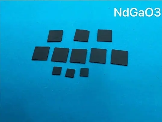
NdGaO3 Substrate
NdGaO3 is a new type of substrate developed in the past decade, mainly used as a substrate for epitaxial film growth of high-temperature superconductors (such as YBCO) and magnetic materials. Because the lattice mismatch between NdGaO3 and YBCO is very small (~0.27%), and there is no structural phase change, a good quality film can be epitaxially grown on the NdGaO3 substrate. OST Photonics offers high quality NdGaO3...
- ManufacturerOST Photonics
- CategoryCrystal Wafer and Substrate
- Lead TimeQuoted per order
- CustomizationSize, orientation and surface finish to drawing
NdGaO3 is a new type of substrate developed in the past decade, mainly used as a substrate for epitaxial film growth of high-temperature superconductors (such as YBCO) and magnetic materials. Because the lattice mismatch between NdGaO3 and YBCO is very small (~0.27%), and there is no structural phase change, a good quality film can be epitaxially grown on the NdGaO3 substrate.
OST Photonics offers high quality NdGaO3 substrates for researchers and industries. Crystal orientation, size and thickness can be customized according to your requirements.
Features
- Small lattice mismatch between NdGaO3 and YBCONo structural phase change
Applications
- Substrate material for high-temperature superconductors (such as YBCO) filmSubstrate material for magnetic film
Processing Capability
- Orientation: <100>,<110>,<111>, etc.Dimension: 10x3mm, 10x5mm, 10x10mm, 15x15mm, 20x15mm, 20x20mm, etc.Thickness: 0.5mm, 1.0mm, etc.Available items: substrates, blanks and customized optics
Specification and properties of NdGaO3 Substrates
| Crystal Structure | Orthogonal |
| Lattice Constant | a=5.43 Å, b=5.50 Å, c=7.71 Å |
| Melting point | 1600 ℃ |
| Density | 7.57 g/cm3 |
| Dielectric Constants | ε= 25 |
| Growth Method | Czochralski |
| Orientation | <100>,<110>,<111>, etc. |
| Orientation Tolerance | ±0.5° or better |
| Dimension | 10x3mm, 10x5mm, 10x10mm, 15x15mm, 20x15mm, 20x20mm, etc. |
| Dimension Tolerance | ±0.1 mm or better |
| Thickness | 0.5mm, 1.0mm, etc. |
| Thickness Tolerance | ±0.05 mm or better |
| Surface Finish | Single side polished (SSP)/Double sides polished (DSP) |
| Surface Roughness | Ra≤5Å (5µmx5µm) |
| Package | Class 100 clean bag, Class 1000 super clean room |
Other Crystal Wafer and Substrate Materials


Request A Quote For NdGaO3 Substrate
Send us your dimensions, orientation, surface finish and quantity. Our engineers reply with a technical proposal and price.
Buyer Questions
What is the crystal structure of the NdGaO3 Substrate?
What is the lattice constant of the NdGaO3 Substrate?
What is the melting point of the NdGaO3 Substrate?
What is the density of the NdGaO3 Substrate?
How do I get a quotation for the NdGaO3 Substrate?
Can the NdGaO3 Substrate be made to a custom specification?
Who manufactures the NdGaO3 Substrate?
Tell Us What You Need
Send your specification, quantity and destination port. Our engineers reply with a technical proposal and a confirmed lead time.